
Nanotechnology
About the course
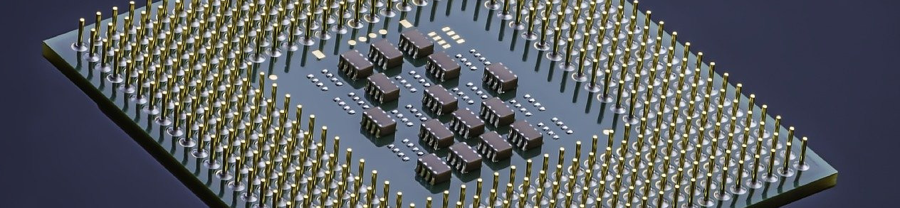
Nanotechnology is an advanced course on the technological, physical and chemical methods used in modern semiconductor nanoelectronics fabrication. This subject will bring the students more towards the development of chips, will bring out the detailed analysis how actual fabrication works and what all processes and methods are involved in the development of a chip design from scratch. Along with theoretical teaching of each such aspect, students will have the opportunity to perform laboratory sessions, where students will explore and work in the environment of clean room. Development of nano level, fabrication of FET devices and careful measurement and characterization of fabricated devices are some of the domains, students will work on. The theoretical teaching will included complete study of modern processes with all necessary understanding of the advanced fabrication processes.
Curriculum
The students will be able to
1. Describe the technological processes involved
a. fabrication of nano & microelectronic devices
2. Compare alternative fabrication methods
3. Apply the knowledge to specific device needs
4. Assess pros & cons of multiple fabrication methods
5. Combine fabrication methods to develop complex processs
a. functional devices and circuits in a range of applications
i. e.g. transistors, solar cells, optoelectronics..
Credit hours
Exam credits: Written examination (50%), lab course and tutorial (50%). Both parts must be passed separately. Written examination requires passing the lab-course.
Your Instructor

Prof. Dr.-Ing. Peter Haring Bolívar
room:
H-E 307
phone:
+49 (271) 740-2157
mail:
peter.haring@uni-siegen.de
Universität Siegen
Lehrstuhl Höchstfrequenztechnik und Quantenelektronik